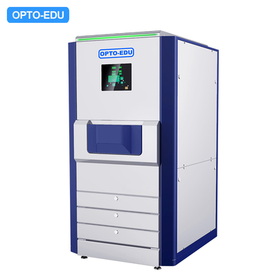
OPTO-EDU A63.7235 High-Throughput Field Emission Scanning Electron Microscope 12KV 600000x
-
Highlight
Field Emission Scanning Electron Microscope 12KV
,High-Throughput Scanning Microscope 600000x
,OPTO-EDU SEM with high magnification
-
Electron GunSchottky Type Thermal Field Emission Electron Source Beam Current Stability <1%/day
-
Objective Lens SystemSORRIL™ Electromagnetic Compound Lens Sample Stage Deceleration Mode
-
Standard Working Distance1.5mm
-
Maximum Field Of View100um (Standard Working Distance) 1mm (Maximum Working Distance)
-
Electron Detector (Standard)In-column SE Detector In-lens BSE Detector
-
W.D. Height DetectionFocus Tracking™ Automatic Focus Tracking System
-
Place of OriginChina
-
Brand NameCNOEC, OPTO-EDU
-
CertificationCE, Rohs
-
Model NumberA63.7230
-
Document
-
Minimum Order Quantity1 pc
-
PriceFOB $1~1000, Depend on Order Quantity
-
Packaging DetailsCarton Packing, For Export Transportation
-
Delivery Time5~20 Days
-
Payment TermsT/T,West Union,Paypal
-
Supply Ability5000 pcs/ Month
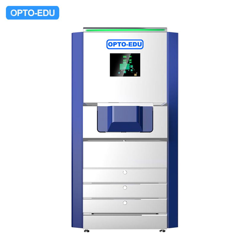
OPTO-EDU A63.7235 High-Throughput Field Emission Scanning Electron Microscope 12KV 600000x

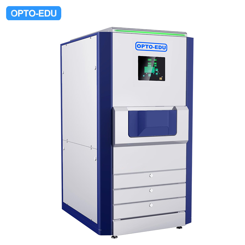
OPTO-EDU A63.7235 High-Throughput Field Emission Scanning Electron Microscope 12KV 600000x
Key Features
- Resolution 1.5nm@1Kv, Automatic Acquisition Stitching Large Image Upto cm2 Size
- Dual-channel Synchronous Imaging of SE And BSE Each 100M Pixels/s
- Comprehensive Imaging Speed > 10 Times That of Traditional Electron Microscopes
- Rapid Generation of Data Analysis Reports From Massive SEM Images
- Cross-scale Material Characterization From Millimeters to Nanometers
The A63.7235 High-Throughput Field Emission Scanning Electron Microscope is designed for cross-scale large-scale sample SEM characterization and analysis, widely used in research and industry. Its automated ultra-high-speed nano imaging technology provides an extraordinary imaging experience.
Core Capabilities:
- Resolution 1.5nm@1Kv, Automatic Acquisition Stitching Large Image Up to cm2 Size
- Dual-channel Synchronous Imaging of SE And BSE Each 100M Pixels/s
- Comprehensive Imaging Speed > 10 Times That of Traditional Electron Microscopes
- Rapid Generation of Data Analysis Reports From Massive SEM Images
- Cross-scale Material Characterization From Millimeters to Nanometers
The A63.7235 High-Throughput Field Emission Scanning Electron Microscope, independently developed by Opto-Edu, achieves high-throughput imaging through systematic innovative design in imaging technology, motion platform, circuit control, and intelligent algorithms, with imaging speeds exceeding traditional electron microscopes by dozens of times. It adopts direct electron detectors, overcoming limitations of traditional SEM technology in speed, accuracy, and sample damage.
Technical Specifications
| Electron Optical Lens | |
|---|---|
| Electron Gun | Schottky Type Thermal Field Emission Electron Source Beam Current Stability <1%/day |
| Objective Lens System | SORRIL™ Electromagnetic Compound Lens Sample Stage Deceleration Mode |
| Resolution | 1.5 nm @ 1kV 1.3nm @ 3kV |
| Immersion Electromagnetic Lens (*①) | |
| Acceleration Voltage | 0.1-12 kV Continuously Adjustable (*②) |
| Magnification | 500X~600,000X (SEM Image) 1X-600X (Optical Navigation) |
| Beam Current | 50pA~30nA (*③) |
| Standard Working Distance | 1.5mm |
| Maximum Field of View | 100um (Standard Working Distance) 1mm (Maximum Working Distance) |
| Electron Beam Blanker | Electrostatic Blanker |
Advanced Features
▶ Ultra-fast Imaging
- Achieved dual-channel synchronous imaging of secondary electrons and backscattered electrons through independently developed hardware and software design: video-level high-resolution imaging
- High-definition video-level frame rate allows real-time observation of sample dynamic changes
▶ High Imaging Quality
- Unique immersion electromagnetic compound lens system effectively reduces optical aberrations
- Electrostatic scanning deflection system reduces image edge distortion
- In-Lens SE and BSE semiconductor direct electron detectors enable dual-channel simultaneous high-speed imaging
- Active compensation system eliminates environmental interference
▶ Cross-Scale Large-Scale Imaging
- Ultra-high-speed scanning imaging capability with fully automatic focusing tracking system
- A.I. image processing algorithms enable high-resolution fully automatic uninterrupted matrix scanning
- Automatically stitching to obtain large-size nanometer-level resolution panoramic imaging
▶ Intelligent Analysis
- Big data intelligent analysis, rapid generation of data analysis reports
- Intelligent image processing, customized image measurement, statistics, and analysis
▶ Simple Operation
- Fully automatic sample loading and navigation, one-click sample replacement
- Large field optical imaging navigation seamlessly connects with SEM imaging
- 24/7 fully automated unmanned operation capability
Application Examples
Observe the microstructure of cells in mouse brain, heart, liver, and kidney under scanning electron microscopy, using Arrays Scan to perform fully automatic scanning on target area samples.
The sample is prepared using a continuous slicing method, collecting up to hundreds of slices, placing them on a sample circle, and loading them into SEM at once.
Pathological Analysis: Comprehensively collect all detailed information on the entire slice, and zoom in on any area to clearly observe the subcellular organelle ultrastructure on the kidney tissue.
Notes
* Note:
①: Optional non-immersion electromagnetic lens for observing ferromagnetic materials
②: Optional 0~30kV electron gun
③: Optional 100nA
④: Optional laser interferometer
①: Optional non-immersion electromagnetic lens for observing ferromagnetic materials
②: Optional 0~30kV electron gun
③: Optional 100nA
④: Optional laser interferometer
Related Products
Our products are sold all over the world, you can rest assured.