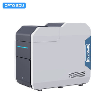
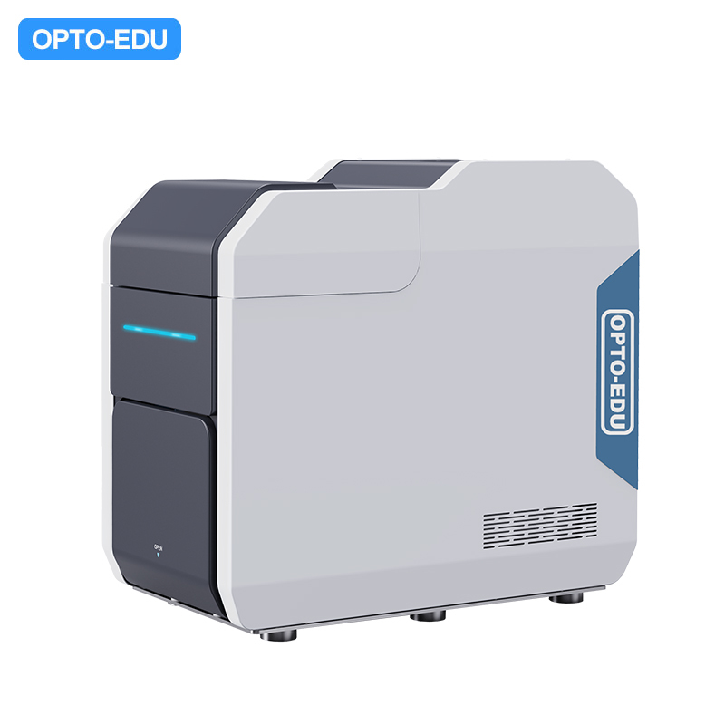
OPTO-EDU A63.7003 Tungsten Filament Scanning Electron Microscope SE BSE 360000x 4nm@20KV
-
Resolution4nm@20KV
-
Magnification360000x
-
Electron GunTungsten
-
Voltage3-20KV
-
DetectorBSE+SE
-
Navigation CCDCCD+Cabin Camera
-
Place of OriginChina
-
Brand NameCNOEC, OPTO-EDU
-
CertificationCE, Rohs
-
Model NumberA63.7003
-
Document
-
Minimum Order Quantity1 pc
-
PriceFOB $1~1000, Depend on Order Quantity
-
Packaging DetailsCarton Packing, For Export Transportation
-
Delivery Time5~20 Days
-
Payment TermsT/T, West Union, Paypal
-
Supply Ability5000 pcs/ Month
OPTO-EDU A63.7003 Tungsten Filament Scanning Electron Microscope SE BSE 360000x 4nm@20KV
|
A63.7003 Desktop Scanning Electron Microscopes (SEM) incorporate numerous innovative technologies, offering not only excellent imaging performance but also portability, catering to a wide range of application needs. Both domestically and internationally, the ZEM series, with its high-end positioning and diverse models, has achieved advanced standards in imaging clarity, user-friendliness, and system integration.
A63.7003 is renowned for its high level of integration and flexible configuration options. The user interface is simple, easy to learn, and operate, allowing even non-expert users to quickly become proficient. The accompanying software supports the entire workflow, from sample preparation, parameter adjustment, to image analysis, providing an integrated and efficient solution. A63.7003 has demonstrated strong analytical capabilities across multiple fields such as new materials, new energy, biomedicine, and semiconductors, assisting researchers in exploring the mysteries of the microscopic world. Due to its excellent cost-performance ratio, the ZEM series has become a preferred choice for many universities, research institutions, and enterprises seeking a desktop scanning electron microscope.
The A63.7003 benchtop SEM utilizes a wider range of accelerating voltages, 1Kvsteps, and a maximum magnification of 360,000x with a resolution of up to 5nmThe tabletop deceleration mode allows real-time observation of low-conductivity products without the need for gold spraying. The extra-large sample compart-ment can be integrated with a wide range of in-situ expansion platforms to meet different experimental and inspection needs. |
|
Working Conditions: Environmental requirements: small size, the whole machine can be placed on an ordinary laboratory table, no need to be equipped with an additional shock absorbing table. 1.Power supply 220V, 50Hz, 1KW 2.Temperature: Operating ambient temperature: 15°C-30°C 3.Humidity: <80%RH |
|
Main Specification: 1. Acceleration voltage: 3-20kV, continuously adjustable. 2. Electron gun type: pre-aligned tungsten filament, life time 100 hours, easy to replace by user, highly integrated two-stage gun lens, no need to manually adjust the diaphragm of the objective lens. 3. Magnification ≥360000X; 4. Resolution:≤4nm@20KV 5. Detector: secondary electron detector (SE), quadruple backscatter detector (BSE), 6. Stage: 2 Axis XY motorized stage, moving 60x55mm; 7. Maximum sample size: 100*78*68.5mm while XY axes move freely 8. Sample change and high vacuum pumping time≤ 30s. 9. High vacuum system: built-in turbo molecular pump, external mechanical pump, the vacuum in sample chamber ≥1x10⁻¹Pa, fully automatic control; 10. Video mode ≥512x512 pixels, no need for small window scanning. 11. Quick scan mode: imaging time≤3s, 512x512 pixels. 12. Slow scan mode: imaging time≤40s, 2048x2048 pixels. 13. Image File: BMP, TIFF, JPEG, PNG. 14. One-key automatic adjustment of brightness and contrast, auto-focus, large image stitching 15. Navigation function: optical camera navigation and cabin camera. 16. Image measurement function: distance, angle, etc. 17. Including computer & software, mouse control. 18. Optional: --Tungsten filament (20pcs/box) --EDS --3 Axis Motorized Stage XYZ --3 Axis Motorized Stage XYT --5 Axis Motorized Stage XYZRT --Low vacuum (1-100Pa) --Deceleration Mode, 1-10KV, can observe non-conductor or poor conductivity samples without gold spraying, only for BSE mode --In-Situ stage from original factory, heating, cooling, stretch, etc. --Shock-absorbing Platform (recommend for A63.7003) 19.Microscope size 650*370*642mm, mechanical pump size 340*160*140mm |
| Model | A63.7001 | A63.7002 | A63.7003 | A63.7004 | A63.7005 |
| Resolution | 10nm@15KV | 6nm@18KV | 4nm@20KV | 3nm@20KV | 2.5nm@15KV |
| Magnification | 150000x | 200000x | 360000x | 360000x | 1000000x |
| Electron Gun | Tungsten | Tungsten | Tungsten | LaB6 | Schotty FEG |
| Voltage | 5/10/15KV | 3-18KV | 3-20KV | 3-20KV | 1-15KV |
| Detector | BSE+SE | BSE+SE | BSE+SE | BSE+SE | BSE+SE |
| Navigation CCD | CCD | CCD | CCD+Cabin Camera | CCD+Cabin Camera | CCD+Cabin Camera |
| Vaccum Time | 90s | 90s | 30s | 90s | 180s |
| Vaccum System | Mechanical Pump Molecular Pump |
Mechanical Pump Molecular Pump |
Mechanical Pump Molecular Pump |
Mechanical Pump Molecular Pump Ion Pump |
Mechanical Pump Molecular Pump Ion Pump x2 |
| Vaccum | High Vaccum 1x10⁻¹Pa |
High Vaccum 1x10⁻¹Pa |
High Vaccum 1x10⁻¹Pa |
High Vaccum 5x10⁻⁴Pa |
High Vaccum 5x10⁻⁴Pa |
| Stage | XY Stage, 40x30/40x40mm |
XY Stage, 40x30/40x40mm |
XY Stage, 60x55mm |
XY Stage, 60x55mm |
XY Stage, 60x55mm |
| Stage Precision | - | Position Precise 5um | |||
| Working Distance | 5-35mm | 5-35mm | 5-73.4mm | 5-73.4mm | 5-73.4mm |
| Max Specimen | 80x42x40mm | 80x42x40mm | 100x78x68.5mm | 100x78x68.5mm | 100x78x68.5mm |
| Optional | Tungsten Filament 20 pcs/box | Lab6 Filament | Field Emission Lamp | ||
| EDS Oxford AZtecOne with XploreCompact 30 | |||||
| - | Low Vaccum 1-100Pa | Low Vaccum 1-30Pa | |||
| - | Z Axis Module | 3 Axis Stage, X 60mm, Y 50mm, Z 25mm | |||
| - | T Axis Module | 3 Axis Stage, X 60mm, Y 50mm, T ±20° | |||
| - | - | 5 Axis Stage, X 90mm, Y 50mm, Z 25mm, T ±20°, R 360° | |||
| - | - | Shock-absorbing Platform, For 3 Axis, 5 Axis Stage | |||
| - | Deceleration Mode 1-10KV To Watch Non-conduct Samples, Only For BSE | ||||
| - | In-Situ Stage From Original Factory, Heating, Cooling, Stretch, etc. | ||||
| UPS | |||||
|
▶ AZtecOne with XploreCompact 30 for TTM
System Conventional Eds Analysis The system provides qualitative and quantitative analysis of different materials, analyzing elements ranging from B(5) to cf (98).in addition to individual point scans of the sample surface, powerful line scans and elemental spec-tral scans are also available. combined with a customized detector, analysis and reporting can be done in seconds. |
| Effective Crystal Area | 30mm2 | Resolution (Of A Photo) | Mn Ka <129eV @50,000cps |
| Elemental Detection Range | B (5) to cf (98) | Maximum Input Count Rate | >1,000,000 cps |
Our products are sold all over the world, you can rest assured.