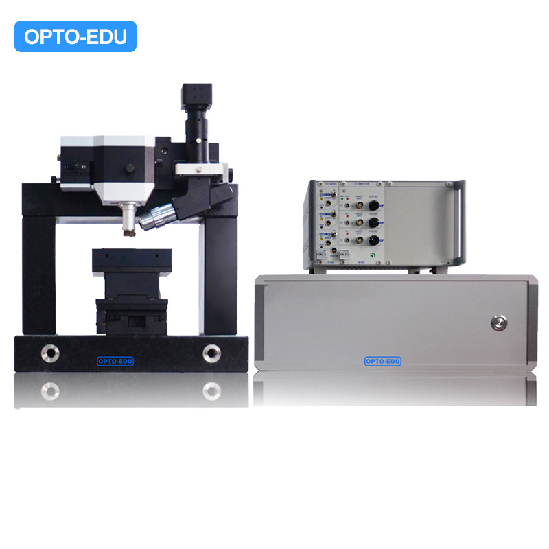
Plane Scanning Atomic Force Microscope
- Gantry scanning head design, marble base, vacuum adsorption stage, sample size and weight are basically unlimited
- A62.4510 + Closed-loop three-axis independent pressure shift scanner, which can scan with high precision in a wide range
- Intelligent needle feeding method with automatic detection of motor-controlled piezoelectric ceramics to protect probes and samples
- Automatic optical positioning, no need to adjust focus, real-time observation and positioning probe sample scanning area
- Equipped with closed metal shield, pneumatic shock-absorbing table, strong anti-interference ability
◆ The first commercial atomic force microscope in China to realize combined mobile scanning of probe and sample;
◆ The first in China to use a three-axis independent closed-loop piezoelectric shift scanning table to achieve large-scale high-precision scanning;
◆ Three-axis independent scanning, XYZ does not affect each other, very suitable for three-dimensional material and topography detection;
◆ Electric control of sample moving table and lifting table, which can be programmed with multi-point position to realize fast automatic detection;
◆ Gantry scanning head design, marble base, vacuum adsorption and magnetic adsorption stage;
◆ The motor automatically controls the intelligent needle feeding method of the piezoelectric ceramic automatic detection to protect the probe and the sample;
◆ High magnification auxiliary optical microscope positioning, real-time observation and positioning of probe and sample scanning area;
◆ The closed-loop piezoelectric scanning stage does not require nonlinear correction, and the nanometer characterization and measurement accuracy is better than 99.5%.

-
| |
A62.4510 |
A62.4511 |
| Work Mode |
Contact Mode
Tapping Mode
【Optional】
Friction Mode
Phase Mode
Magnetic Mode
Electrostatic Mode |
Contact Mode
Tapping Mode
【Optional】
Friction Mode
Phase Mode
Magnetic Mode
Electrostatic Mode |
| Current Spectrum Curve |
RMS-Z Curve
F-Z Force Curve |
RMS-Z Curve
F-Z Force Curve |
| XY Scan Mode |
Probe Driven Scanning,
Piezo Tube Scanner |
Sample Driven Scanning, Closed Loop Piezoelectric Shift Scanning Stage |
| XY Scan Range |
70×70um |
Closed Loop 100×100um |
| XY Scan Resolution |
0.2nm |
Closed Loop 0.5nm |
| Z Scan Mode |
|
Probe Driven Scanning |
| Z Scan Range |
5um |
5um |
| Z Scan Resolution |
0.05nm |
0.05nm |
| Scan Speed |
0.6Hz~30Hz |
0.6Hz~30Hz |
| Scan Angle |
0~360° |
0~360° |
| Sample Weight |
≤15Kg |
≤0.5Kg |
| Stage Size |
Dia.100mm
【Optional】
Dia.200mm
Dia.300mm |
Dia.100mm
【Optional】
Dia.200mm
Dia.300mm |
| Stage XY Moving |
100x100mm, Resolution 1um
【Optional】
200x200mm
300x300mm |
100x100mm, Resolution 1um
【Optional】
200x200mm
300x300mm |
| Stage Z Moving |
15mm, Resolution 10nm
【Optional】
20mm
25mm |
15mm, Resolution 10nm
【Optional】
20mm
25mm |
| Shock-Absorbing Design |
Spring Suspension
【Optional】
Active Shock Absorber |
Spring Suspension
【Optional】
Active Shock Absorber |
| Optical System |
Objective 5x
5.0M Digital Camera
【Optional】
Objective 10x
Objective 20x |
Objective 5x
5.0M Digital Camera
【Optional】
Objective 10x
Objective 20x |
| Output |
USB2.0/3.0 |
USB2.0/3.0 |
| Software |
Win XP/7/8/10 |
Win XP/7/8/10 |
| Main Body |
Gantry Scan Head, Marble Base |
Gantry Scan Head, Marble Base |
-
| Microscope |
Optical Microscope |
Electron Microscope |
Scanning Probe Microscope |
| Max Resolution (um) |
0.18 |
0.00011 |
0.00008 |
| Remark |
Oil immersion 1500x |
Imaging diamond carbon atoms |
Imaging high-order graphitic carbon atoms |
|
|
|
-
| Probe-Sample Interaction |
Measure Signal |
Information |
| Force |
Electrostatic Force |
Shape |
| Tunnel Current |
Current |
Shape, Conductivity |
| Magnetic Force |
Phase |
Magnetic Structure |
| Electrostatic Force |
Phase |
charge distribution |
-
| |
Resolution |
Working Condition |
Working Temperation |
Damge to Sample |
Inspection Depth |
| SPM |
Atom Level 0.1nm |
Normal, Liquid, Vacuum |
Room or Low Temperation |
None |
1~2 Atom Level |
| TEM |
Point 0.3~0.5nm
Lattice 0.1~0.2nm |
High Vaccum |
Room Temperation |
Small |
Usually <100nm |
| SEM |
6-10nm |
High Vaccum |
Room Temperation |
Small |
10mm @10x
1um @10000x |
| FIM |
Atom Level 0.1nm |
Super High Vaccum |
30~80K |
Damge |
Atom Thickness |
-
-
-