Send Message
Opto-Edu (Beijing) Co., Ltd. 0086-13911110627 sale@optoedu.com
Opto Edu A62.4510 Electron Probe Microscope , Spm Microscope Usb

Opto Edu A62.4510 Electron Probe Microscope , Spm Microscope Usb

  • High Light

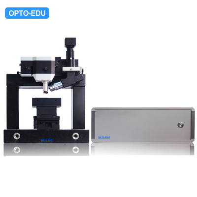
    opto edu electron probe microscope

    ,

    usb electron probe microscope

    ,

    opto edu spm microscope

  • Work Mode
    "Contact Mode Tapping Mode 【Optional】 Friction Mode Phase Mode Magnetic Mode Electrostatic Mode"
  • Current Spectrum Curve
    "RMS-Z Curve F-Z Force Curve"
  • XY Scan Mode
    "Probe Driven Scanning, Piezo Tube Scanner"
  • XY Scan Range
    70×70um
  • XY Scan Resolution
    0.2nm
  • Z Scan Range
    5um
  • Z Scan Resolution
    0.05nm
  • Scan Speed
    0.6Hz~30Hz
  • Scan Angle
    0~360°
  • Sample Weight
    ≤15Kg
  • Stage Size
    "Dia.100mm 【Optional】 Dia.200mm Dia.300mm"
  • Stage XY Moving
    " 100x100mm, Resolution 1um 【Optional】 200x200mm 300x300mm"
  • Stage Z Moving
    "15mm, Resolution 10nm 【Optional】 20mm 25mm"
  • Shock-Absorbing Design
    "Spring Suspension 【Optional】 Active Shock Absorber"
  • Optical System
    "Objective 5x 5.0M Digital Camera 【Optional】 Objective 10x Objective 20x"
  • Place of Origin
    China
  • Brand Name
    OPTO-EDU
  • Certification
    CE, Rohs
  • Model Number
    A62.4510
  • Minimum Order Quantity
    1pc
  • Price
    FOB $1~1000, Depend on Order Quantity
  • Packaging Details
    Carton Packing, For Export Transportation
  • Delivery Time
    5~20 Days
  • Payment Terms
    L/C, T/T, Western Union
  • Supply Ability
    5000 pcs/ Month

Opto Edu A62.4510 Electron Probe Microscope , Spm Microscope Usb

Probe Scanning Atomic Force Microscope

  • Gantry scanning head design, marble base, vacuum adsorption stage, sample size and weight are basically unlimited
  • Intelligent needle feeding method with automatic detection of motor-controlled piezoelectric ceramics to protect probes and samples
  • Automatic optical positioning, no need to adjust focus, real-time observation and positioning probe sample scanning area
  • Equipped with closed metal shield, pneumatic shock-absorbing table, strong anti-interference ability;
  • Integrated scanner nonlinear correction user editor, nanometer characterization and measurement accuracy is better than 98%
  • Opto Edu A62.4510 Electron Probe Microscope , Spm Microscope Usb 0
  • Opto Edu A62.4510 Electron Probe Microscope , Spm Microscope Usb 1
  •            ◆ The first commercial atomic force microscope in China that keeps the sample stationary and the probe moves and scans;

               ◆ The sample size and weight are almost unlimited, especially suitable for the detection of very large samples;

  •            ◆ The sample stage is highly expandable, which is very convenient for multi-instrument combination to realize in-situ detection;

               ◆ Electric control of sample moving table and lifting table, which can be programmed with multi-point position to realize fast automatic detection;

               ◆ Gantry scanning head design, marble base, vacuum adsorption and magnetic adsorption stage;

  •           ◆ The motor automatically controls the intelligent needle feeding method of the piezoelectric ceramic automatic detection to protect the probe and the sample;

  •           ◆ High magnification auxiliary optical microscope positioning, real-time observation and positioning of probe and sample scanning area;

  •           ◆ Integrated scanner nonlinear correction user editor, nanometer characterization and measurement accuracy better than 98%.

  • Opto Edu A62.4510 Electron Probe Microscope , Spm Microscope Usb 2

  •  

  • Opto Edu A62.4510 Electron Probe Microscope , Spm Microscope Usb 3
  •   A62.4510 A62.4511
    Work Mode Contact Mode
    Tapping Mode

    【Optional】
    Friction Mode
    Phase Mode
    Magnetic Mode
    Electrostatic Mode
    Contact Mode
    Tapping Mode

    【Optional】
    Friction Mode
    Phase Mode
    Magnetic Mode
    Electrostatic Mode
    Current Spectrum Curve RMS-Z Curve
    F-Z Force Curve
    RMS-Z Curve
    F-Z Force Curve
    XY Scan Mode Probe Driven Scanning,
    Piezo Tube Scanner
    Sample Driven Scanning, Closed Loop Piezoelectric Shift Scanning Stage
    XY Scan Range 70×70um Closed Loop 100×100um
    XY Scan Resolution 0.2nm Closed Loop 0.5nm
    Z Scan Mode   Probe Driven Scanning
    Z Scan Range 5um 5um
    Z Scan Resolution 0.05nm 0.05nm
    Scan Speed 0.6Hz~30Hz 0.6Hz~30Hz
    Scan Angle 0~360° 0~360°
    Sample Weight ≤15Kg ≤0.5Kg
    Stage Size Dia.100mm

    【Optional】
    Dia.200mm
    Dia.300mm
    Dia.100mm

    【Optional】
    Dia.200mm
    Dia.300mm
    Stage XY Moving 100x100mm, Resolution 1um

    【Optional】
    200x200mm
    300x300mm
    100x100mm, Resolution 1um

    【Optional】
    200x200mm
    300x300mm
    Stage Z Moving 15mm, Resolution 10nm
    【Optional】
    20mm
    25mm
    15mm, Resolution 10nm
    【Optional】
    20mm
    25mm
    Shock-Absorbing Design Spring Suspension

    【Optional】
    Active Shock Absorber
    Spring Suspension

    【Optional】
    Active Shock Absorber
    Optical System Objective 5x
    5.0M Digital Camera

    【Optional】
    Objective 10x
    Objective 20x
    Objective 5x
    5.0M Digital Camera

    【Optional】
    Objective 10x
    Objective 20x
    Output USB2.0/3.0 USB2.0/3.0
    Software Win XP/7/8/10 Win XP/7/8/10
    Main Body Gantry Scan Head, Marble Base Gantry Scan Head, Marble Base
  • Microscope Optical Microscope Electron Microscope Scanning Probe Microscope
    Max Resolution (um) 0.18 0.00011 0.00008
    Remark Oil immersion 1500x Imaging diamond carbon atoms Imaging high-order graphitic carbon atoms
    Opto Edu A62.4510 Electron Probe Microscope , Spm Microscope Usb 4   Opto Edu A62.4510 Electron Probe Microscope , Spm Microscope Usb 5
  • Probe-Sample Interaction Measure Signal Information
    Force Electrostatic Force Shape
    Tunnel Current Current Shape, Conductivity
    Magnetic Force Phase Magnetic Structure
    Electrostatic Force Phase charge distribution
  •   Resolution Working Condition Working Temperation Damge to Sample Inspection Depth
    SPM Atom Level 0.1nm Normal, Liquid, Vacuum Room or Low Temperation None 1~2 Atom Level
    TEM Point 0.3~0.5nm
    Lattice 0.1~0.2nm
    High Vaccum Room Temperation Small Usually <100nm
    SEM 6-10nm High Vaccum Room Temperation Small 10mm @10x
    1um @10000x
    FIM Atom Level 0.1nm Super High Vaccum 30~80K Damge Atom Thickness
  • Opto Edu A62.4510 Electron Probe Microscope , Spm Microscope Usb 6
  •  
  •  
  •