
Opto Edu Teaching Level Atomic Force Microscope with 20×20um XY Scan Range 0.2nm Resolution and 2.5um Z Scan Range
-
Highlight
teaching opto edu microscope
,tapping mode opto edu microscope
-
Work Mode"Tapping Mode 【Optional】 Contact Mode Friction Mode Phase Mode Magnetic Mode Electrostatic Mode"
-
Current Spectrum Curve"RMS-Z Curve 【Optional】 F-Z Force Curve"
-
XY Scan Range20×20um
-
XY Scan Resolution0.2nm
-
Z Scan Range2.5um
-
Y Scan Resolution0.05nm
-
Scan Speed0.6Hz~30Hz
-
Scan Angle0~360°
-
Sample Size"Φ≤90mm H≤20mm"
-
Shock-Absorbing DesignSpring Suspension
-
Optical Syestem"4x Objective Resolution 2.5um"
-
OutputUSB2.0/3.0
-
SoftwareWin XP/7/8/10
-
Place of OriginChina
-
Brand NameOPTO-EDU
-
CertificationCE, Rohs
-
Model NumberA62.4500
-
Document
-
Minimum Order Quantity1pc
-
PriceFOB $1~1000, Depend on Order Quantity
-
Packaging DetailsCarton Packing, For Export Transportation
-
Delivery Time5~20 Days
-
Payment TermsL/C,T/T,Western Union
-
Supply Ability5000 pcs/ Month
Opto Edu Teaching Level Atomic Force Microscope with 20×20um XY Scan Range 0.2nm Resolution and 2.5um Z Scan Range
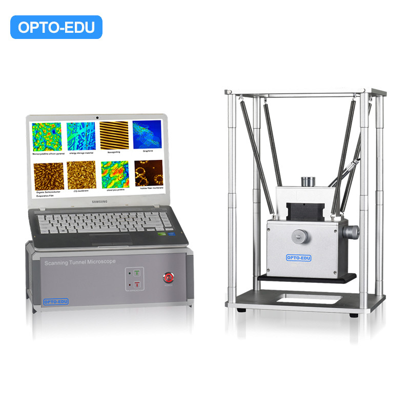
A62.4500 Opto Edu Microscope Tapping Mode Rms-Z Curve Teaching Level Atomic Force
Teaching Level Atomic Force Microscope
- Teaching Level Separate controller & main body design with Tapping Mode, 4x Objective, Miniaturized Detachable Design
- Integrated laser detection head and sample scanning stage for stable structure and strong anti-interference
- Motor-controlled pressurized piezoelectric ceramic automatic detection for intelligent needle feeding, protecting both probe and sample
- Automatic optical positioning eliminates the need for manual focusing, enabling real-time observation of probe sample scanning area
- Spring suspension shockproof method provides simple yet effective vibration isolation
Key Features:
- ◆ Precision probe positioning device with easy laser spot alignment adjustment
- ◆ Single-axis drive sample automatically approaches probe vertically for perpendicular needle tip alignment
- ◆ Metal shielded soundproof box with built-in high-precision temperature and humidity sensor for environmental monitoring
- ◆ Integrated scanner nonlinear correction user editor with nanometer characterization accuracy better than 98%
Technical Specifications
| Specification | A62.4500 | A622.4501 | A62.4503 | A62.4505 |
|---|---|---|---|---|
| Work Mode | Tapping Mode 【Optional】 Contact Mode Friction Mode Phase Mode Magnetic Mode Electrostatic Mode |
Contact Mode Tapping Mode 【Optional】 Friction Mode Phase Mode Magnetic Mode Electrostatic Mode |
Contact Mode Tapping Mode 【Optional】 Friction Mode Phase Mode Magnetic Mode Electrostatic Mode |
Contact Mode Tapping Mode 【Optional】 Friction Mode Phase Mode Magnetic Mode Electrostatic Mode |
| Current Spectrum Curve | RMS-Z Curve 【Optional】 F-Z Force Curve |
RMS-Z Curve F-Z Force Curve |
RMS-Z Curve F-Z Force Curve |
RMS-Z Curve F-Z Force Curve |
| XY Scan Range | 20×20μm | 20×20μm | 50×50μm | 50×50μm |
| XY Scan Resolution | 0.2nm | 0.2nm | 0.2nm | 0.2nm |
| Z Scan Range | 2.5μm | 2.5μm | 5μm | 5μm |
| Y Scan Resolution | 0.05nm | 0.05nm | 0.05nm | 0.05nm |
| Scan Speed | 0.6Hz~30Hz | 0.6Hz~30Hz | 0.6Hz~30Hz | 0.6Hz~30Hz |
| Scan Angle | 0~360° | 0~360° | 0~360° | 0~360° |
| Sample Size | Φ≤90mm H≤20mm |
Φ≤90mm H≤20mm |
Φ≤90mm H≤20mm |
Φ≤90mm H≤20mm |
| XY Stage Moving | 15×15mm | 15×15mm | 25×25μm | 25×25μm |
| Shock-Absorbing Design | Spring Suspension | Spring Suspension Metal Shielding Box |
Spring Suspension Metal Shielding Box |
- |
| Optical System | 4x Objective Resolution 2.5μm |
4x Objective Resolution 2.5μm |
4x Objective Resolution 2.5μm |
Eyepiece 10x Infinity Plan LWD APO 5x10x20x50x 5.0M Digital Camera 10" LCD Monitor, With Measuring LED Kohler Illumination Coaxial Coarse & Fine Focusing |
| Output | USB2.0/3.0 | USB2.0/3.0 | USB2.0/3.0 | USB2.0/3.0 |
| Software | Win XP/7/8/10 | Win XP/7/8/10 | Win XP/7/8/10 | Win XP/7/8/10 |
Microscope Technology Comparison
| Microscope | Optical Microscope | Electron Microscope | Scanning Probe Microscope |
|---|---|---|---|
| Max Resolution (μm) | 0.18 | 0.00011 | 0.00008 |
| Remark | Oil immersion 1500x | Imaging diamond carbon atoms | Imaging high-order graphitic carbon atoms |
Probe-Sample Interaction Analysis
| Probe-Sample Interaction | Measure Signal | Information |
|---|---|---|
| Force | Electrostatic Force | Shape |
| Tunnel Current | Current | Shape, Conductivity |
| Magnetic Force | Phase | Magnetic Structure |
| Electrostatic Force | Phase | charge distribution |
Microscope Performance Characteristics
| Resolution | Working Condition | Working Temperature | Damage to Sample | Inspection Depth | |
|---|---|---|---|---|---|
| SPM | Atom Level 0.1nm | Normal, Liquid, Vacuum | Room or Low Temperature | None | 1~2 Atom Level |
| TEM | Point 0.3~0.5nm Lattice 0.1~0.2nm |
High Vacuum | Room Temperature | Small | Usually <100nm |
| SEM | 6-10nm | High Vacuum | Room Temperature | Small | 10mm @10x 1μm @10000x |
| FIM | Atom Level 0.1nm | Super High Vacuum | 30~80K | Damage | Atom Thickness |
Related Products
Our products are sold all over the world, you can rest assured.